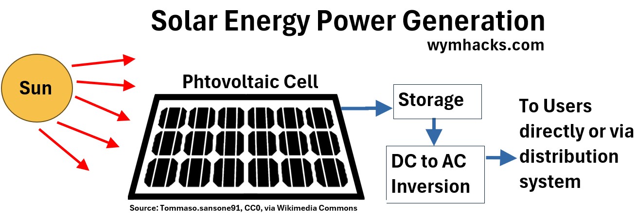
Solar Power Generation
Solar power generation involves converting sunlight into electricity and its energy conversion path is as follows:
Sunlight → DC Electricity→ AC Electricity → Immediate Use / Storage / Into the Grid.
Picture: Solar Power Generation
.
Photovoltaic Effect
Solar panels, made of many smaller units called photovoltaic (PV) cells, receive sunlight.
In a phenomenon called the photovoltaic effect, a particle of sunlight (a photon) hits a PV cell and knocks electrons loose from the material (usually silicon) inside the cell.
An electric field is eventually formed causing these loose electrons to concentrate on one side of the cell and this can be used to generate direct current (DC).
Inversion
To connect to the grid or home, this DC electricity has to be converted to AC (alternating current).
A device called an inverter takes the DC electricity and instantly converts it into usable AC electricity.
Electricity Usage
Once converted to AC power, the electricity can be used in three main ways:
- Direct Use: The electricity is directly supplied to end users.
- Storage: Excess electricity is stored in a battery for later use (e.g. periods where there is no sunlight).
- Grid: Electricity not immediately used or stored can be fed into the main utility grid (the public power lines).
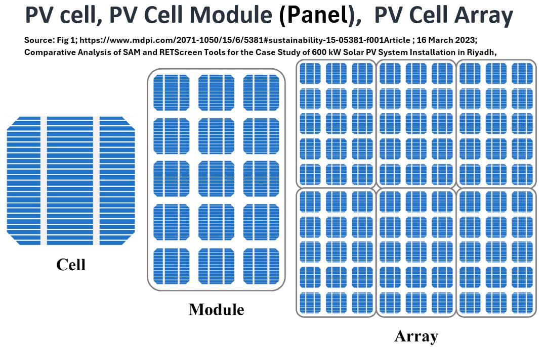
Solar Equipment
A solar power collection system has the following component categories
- the Cell is the base component,
- the Module (Panel) is a collection of cells and
- the Array is a collection of panels.
Picture: Cell, Module, Array
See an example assembly in the picture below.
Picture: Solar Panel (Module) Array
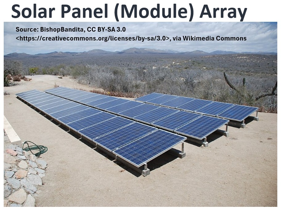
Solar Panel Array
An array is comprised of multiple Solar Modules (commonly called solar panels) mounted together, along with support structures, wiring, and inverters.
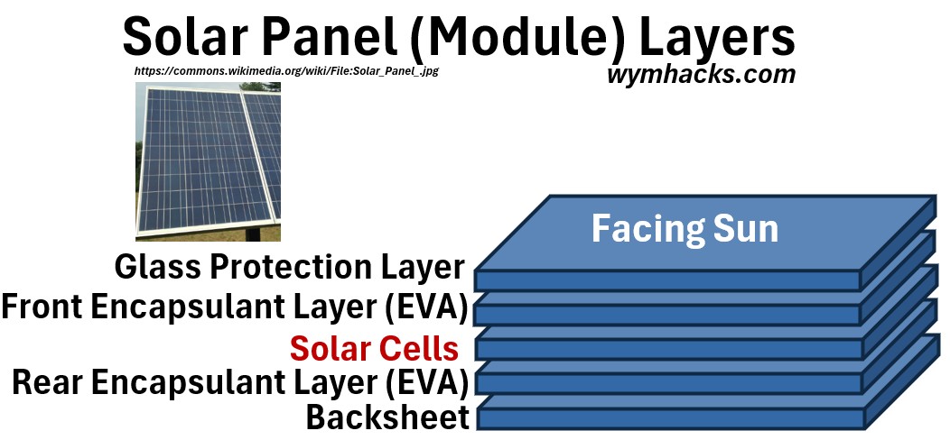
Solar Panel (Module)
A solar module (commonly called a solar panel) is a packaged, weatherproof assembly of many solar cells.
It functions as a robust, packaged assembly of multiple individual solar cells that are electrically connected to achieve a practical voltage and power output (typically 250 to 450 Watts).
To protect these delicate cells, the module is constructed with a highly durable layered structure:
- a top layer of tempered glass for impact resistance,
- 2 layers of EVA encapsulant to seal out moisture and cushion the cells,
- a polymer backsheet for insulation, and
- a strong aluminum frame for structural integrity and ease of mounting.
The purpose of the module is to convert sunlight into a usable quantity of Direct Current (DC) electricity that can be easily wired with other panels to form a larger array.
Picture: Solar Panel (Module) Components (Layers)
Solar Cell
The Solar Cell, or photovoltaic (PV) cell, is the fundamental electronic device responsible for converting light directly into electricity via the photovoltaic effect.
It is typically made from layers of silicon semiconductor material, primarily consisting of
- a positively-doped (p-type) layer and
- a negatively-doped (n-type) layer
- joined at a critical p-n junction.
When photons from sunlight strike the cell, they excite electrons, which are then forced across the junction by a built-in electric field, creating a flow of Direct Current (DC).
To maximize efficiency, the cell surface is often treated with an anti-reflection coating and covered with thin metal contact grids to collect the generated electrons.
Although a single cell produces a very low voltage (around 0.5V to 0.8V), numerous cells are wired together within a solar module to produce a practical, higher voltage and power output.
Picture: Solar Cell Layers
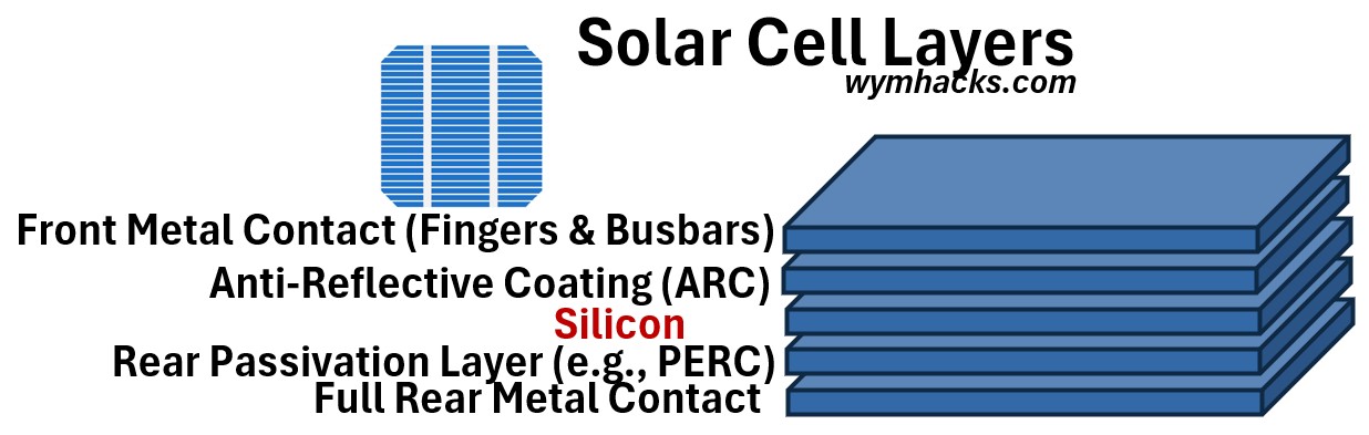
- Top Contact/Conductive Grid (Fingers & Busbars):
- This is a network of thin metal lines (usually silver paste) printed on the front surface.
- It collects the generated electrons and transports the current to the external circuit.
- It’s designed to minimize shading while maximizing conductivity.
Anti-Reflection Coating (ARC):
- A thin layer (often silicon nitride) applied directly over the silicon.
- It reduces the reflection of incoming sunlight, allowing more light (photons) to be absorbed by the silicon, thus boosting efficiency.
- The semiconductor layers of a typical solar cell can be described as a three-layer system:
- a p-n junction is sandwiched between the n-type and p-type silicon layers. It is critical to the creation of current.
- The thickest layer, known as the base or bulk layer, forms the central body of the cell and can be either p-type (in a standard cell) or n-type (in a more advanced cell design).
- The opposing, thinner layer, known as the emitter, serves as the top layer (again it can be an n or p type, opposite what the bulk material type is)
- This three-layer configuration establishes the critical internal electric field at the p-n junction interface, which is essential for separating the electrons and holes generated by sunlight and driving them to their respective front and back contacts, thus creating a functional electrical current.
- The Rear Passivation Layer (RPL) is a thin dielectric film applied to the back of a solar cell, and it is a defining feature of PERC (Passivated Emitter and Rear Cell) technology.
- Back Contact: A continuous metal layer (often aluminum) covering the entire back surface of the cell.
- It collects the holes and completes the internal electrical circuit.
Photovoltaic Effect
The photovoltaic effect is the physical process by which a solar cell directly converts light (photons) into electricity.
It occurs when photons strike the semiconductor material, typically silicon, dislodging electrons from their atoms.
A built-in electric field within the cell’s p-n junction then separates these liberated electrons and their corresponding holes, forcing the electrons to flow in one direction and creating an electrical Direct Current (DC).
This current can then be harnessed to power an external load.
It’s worth digging into this a little.
Silicon
The earth’s crust most abundant elements by weight % are:
1 Oxygen O 46.6%
2 Silicon Si 27.7%
3 Aluminum Al 8.1%
4 Iron Fe 5.0%
5 Calcium Ca 3.6%
We see that Silicon is the second most abundant element in the Earth’s crust.
It’s used widely in modern electronics and is by far the most common element used to manufacture solar cells.
The form of silicon most commonly used in electronics and solar power is its pure, solid, crystalline form.
- This structure is a highly ordered, three-dimensional arrangement known as the diamond cubic lattice.
- Its most essential feature is the tetrahedral, covalent bonding of each atom which is illustrated in the simplified drawing below.
Picture: Silicon Crystal Lattice
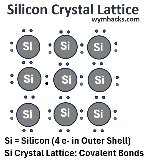
Every silicon atom is symmetrically and strongly bonded to its nearest neighbors in a highly ordered, repeating pattern, which locks the electrons in place.
This pure Silicon is a poor conductor and in this crystal form it is called an intrinsic semiconductor (exhibiting low but measurable conductivity).
p-Type Semiconductor
A p-type semiconductor is created by doping a pure (intrinsic) semiconductor, like silicon, with a small amount of a trivalent impurity (an element with three valence electrons, such as boron).
This doping process introduces a deficiency of electrons at the bond sites, which creates positively charged holes in the material’s crystal lattice.
These holes become the majority charge carriers, allowing the material to conduct electricity primarily through their movement.
Picture: p-Type Semiconductor

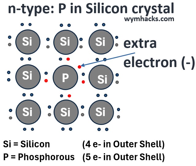
Picture: n-Type Semiconductor
A n-type semiconductor is created by doping an intrinsic semiconductor, like silicon, with a small amount of a pentavalent impurity (an element with five valence electrons, such as phosphorus).
This doping introduces an excess electron into the crystal lattice, which is free to move and carry current.
These electrons become the majority charge carriers, allowing the material to conduct electricity primarily through their movement
The Three Layers in Any Solar Semiconductor Section
A simplified solar cell structure can be understood as having three main parts:
- a thin top layer (the emitter),
- a critical interface layer (the p-n junction) in the middle, and
- a thick bulk layer at the bottom (the base).
The top and bulk layers are fabricated from silicon that is oppositely doped (one p-type and one n-type) to create the interface.
The entire solar cell is ultimately described as either
- a p-type solar cell or an
- n-type solar cell
based on the doping of its bulk layer—the thickest, most substantial part of the device.
note: this is subtle nomenclature you have to keep straight.
- pure Si can be doped with Boron or Phosphorous and
- B doped Si is p-type and P doped Si is n-type
- The bulk layer of the complete semiconductor assembly dictates its name
- So if the bulk layer is n-type, then its an n-type semiconductor
P and N Type Solar Cells
As we’ve noted, solar cells are fundamentally classified by the doping of their thickest, or base, layer:
- the p-type cell, which has been the traditional industry standard, uses boron-doped silicon as its base, resulting in a positive charge due to a dominance of holes (missing electrons).
- In contrast, the n-type cell, which is rapidly becoming the new standard due to its higher efficiency and superior resistance to degradation, uses phosphorus-doped silicon as its base, resulting in a negative charge due to a dominance of free electrons.
Picture: Solar Cell Types
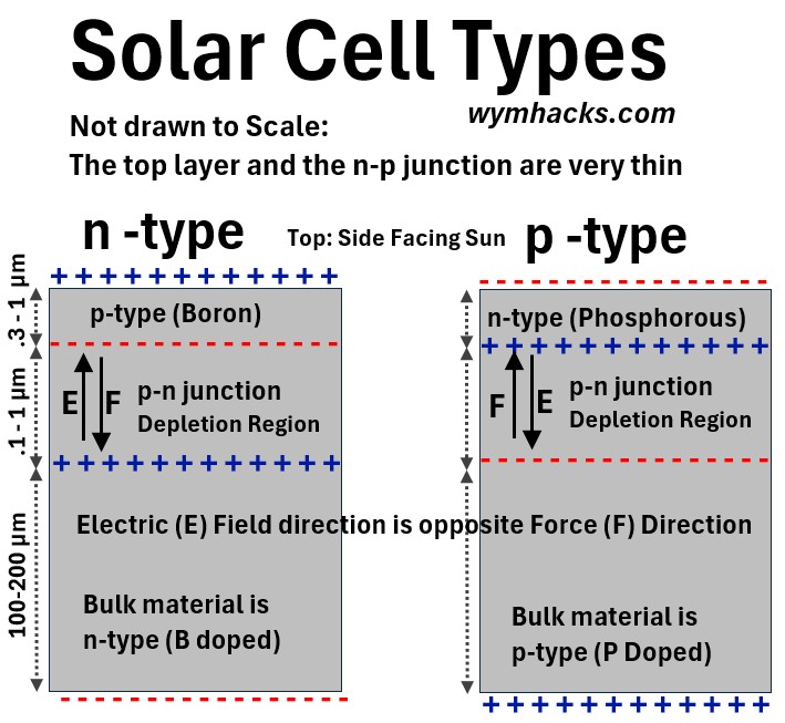
The Depletion Zone in the p-n Junction
In a nutshell:
- The Depletion Zone is critical to the operation.
- It generates an Electric Field which pushes photon loosened electrons to the n-side surface.
- Remember E field points one way, the Force direction will point the other way (this is what pushes the electrons).
- A DC circuit is generated as electrons flow from this negative side to the opposite positive side.
In a little more detail:
The depletion zone is a thin region that forms instantly at the junction between p-type and n-type semiconductor materials.
It generates the electric field necessary for devices like solar cells and diodes to work.
When p-type and n-type silicon are joined, the mobile charges diffuse across the boundary.
Electrons from the n-side fill holes on the p-side, causing them to recombine.
This leaves behind a layer of immobile positive ions (donor atoms) on the n-side and immobile negative ions (acceptor atoms) on the p-side.
Because the free charge carriers (electrons and holes) are quickly swept out or recombined in this region, it is depleted of mobile charges, giving it its name.
The exposed positive and negative fixed charges create a powerful, built-in electric field across the zone.
This field acts as an energy barrier, stopping further diffusion of the majority carriers and establishing equilibrium.
When light strikes the junction, it creates new electron-hole pairs.
The depletion zone’s electric field immediately separates these carriers, pushing the electrons to the n-side and the holes to the p-side, which is the action that generates usable electric current.
The Photoelectric Effect in P-Type and N-Type Solar Cells
In a p-type solar cell, electricity generation is based on the photovoltaic effect occurring at the p-n junction.
- The cell is built with a thick, positive p-type base and a thin, negative n-type emitter on top.
When a photon from sunlight strikes the cell with sufficient energy, it is absorbed and excites an electron, knocking it loose and creating an electron-hole pair.
- The electric field at the p-n junction acts as a one-way barrier: it sweeps the newly freed electrons toward the front (top) n-type layer and the newly created holes toward the back (btm) P-type layer.
This separation of charges creates a voltage, and connecting an external circuit allows the electrons to flow from the n-layer back to the p-layer, generating the useful electrical current.
Picture: Solar Cell Types: n-Type vs p-Type
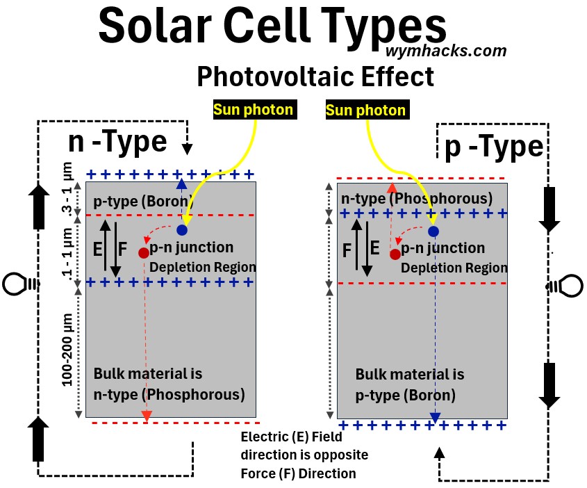
The n-type solar cell works based on the exact same fundamental principle of separating light-generated electron-hole pairs at the p-n junction to produce a current.
However, because its structure is reversed (a thick n-type base and a thin p-type emitter),
- the majority of charge carriers are free electrons in the base layer, and
- the electric field sweeps the electrons in the opposite structural direction compared to the p-type cell.
Despite this internal reversal of charge flow and carrier dominance, the overall result is the same: the photon’s energy is converted into a direct electrical current that flows through the external circuit.
PV Solar Cell Manufacture
The vast majority of solar wafers are manufactured through a four-stage sequence:
- conversion
- purification,
- crystal growth, and
- slicing.
Conversion and Purification:
- Raw silicon is first converted into Trichlorosilane SiHCl3,
- which is then ultra-purified through distillation before
- being decomposed onto heated rods using the Siemens process to yield high-purity polysilicon feedstock.
Crystal Growth:
- The polysilicon is melted and intentionally doped (with Boron or Phosphorous).
- It is then solidified into large blocks or ingots using either
- the Czochralski (CZ) method for single-crystal (mono) silicon or
- the Directional Solidification (DS) method for multi-crystal (multi) silicon.
Wafering:
- The solidified, doped ingots are precisely sliced into extremely thin, square-shaped wafers using multi-wire diamond saws, completing the raw material stage before the final solar cell fabrication begins.
- Wafers are doped (with Phosphorous or Boron) before final fabrication steps occur.
See the process manufacturing flow diagram below.
Picture: PV Cell Manufacturing Process (Simplified)
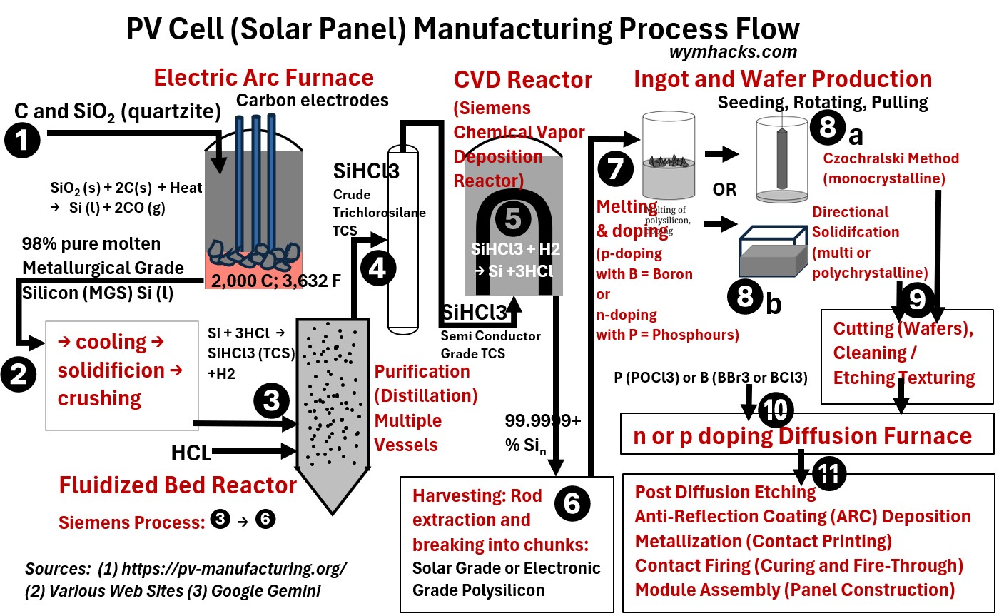
Solar Cell Fabrication Process
The numbers below match the steps shown in the drawing above.
1 React C and Si in an electric arc furnace:
Quartzite SiO2 and carbon (C) are heated to extremely high temperatures (around 1800 – 2000C) to perform a chemical reduction, yielding metallurgical grade silicon (MGS).
2 Metallurgical grade silicon is then cooled, solidified, crushed:
The crude MGS is cooled and physically broken down into smaller pieces to prepare it for the chemical purification stage.
3 Then react the solid Si with HCl in a fluidized bed reactor:
The crushed MGS is reacted with hydrogen chloride gas HCl at high temperatures to produce Trichlorosilane TCS (SiHCl3).
4 TCS produced is purified through distillation:
The liquid TCS is subjected to multiple stages of fractional distillation to remove impurities like boron, iron, and aluminum down to parts-per-billion levels, creating electronic grade silicon.
5 and Routed to a Siemens CVD reactor:
The ultra-pure TCS is decomposed onto heated silicon filaments via Chemical Vapor Deposition (CVD), causing high-purity silicon to deposit slowly.
6 Rod extraction and solid polysilicon nugget formation:
The pure silicon rods are broken into chunks, forming the polycrystalline silicon (poly-Si) material that serves as the basic feedstock.
7 Melting and doping (with B or P):
The poly-Si is melted in a crucible and intentionally mixed with small, precise amounts of a dopant—usually Boron (B) for p-type material or Phosphorus (P) for n-type material.
8a,b CZ method (Czochralski) or Directional Solidification method:
The doped molten silicon is solidified either by pulling a single-crystal ingot (CZ) or by allowing the melt to solidify in a mold to form a multi-crystalline block (DS).
9 Cutting, wafering:
The large silicon ingot or block is sliced into very thin, individual wafers (the base of the solar cell) using multi-wire saws.
10 n or p doping diffusion process:
The wafer is selectively doped in a furnace (e.g., Phosphorus or Boron diffusion) to create the opposing layer and form the crucial p-n junction.
11 Etching, ARC deposition, metallization, contact firing, module assembly:
The wafer is chemically cleaned (etching), coated with an Anti-Reflection Coating (ARC), conductive metal lines are applied (metallization), the metal is sintered to the silicon (contact firing), and finally, the completed cells are connected, encapsulated, and framed into a module (panel).